(China (Mainland))

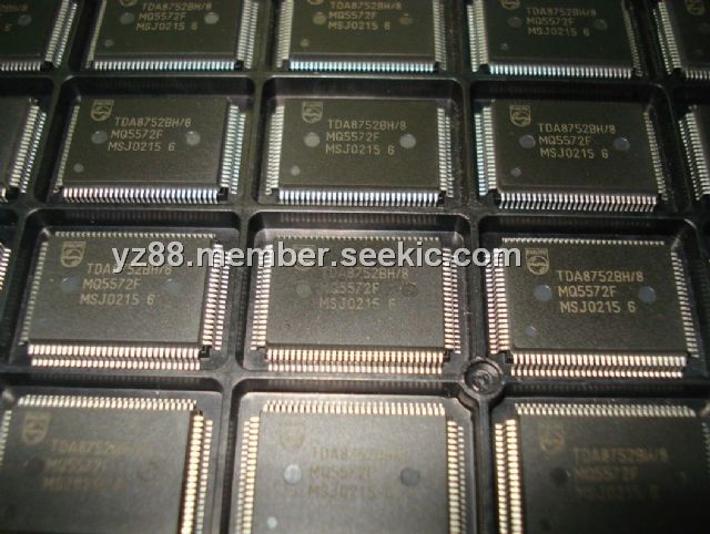
Product Summary
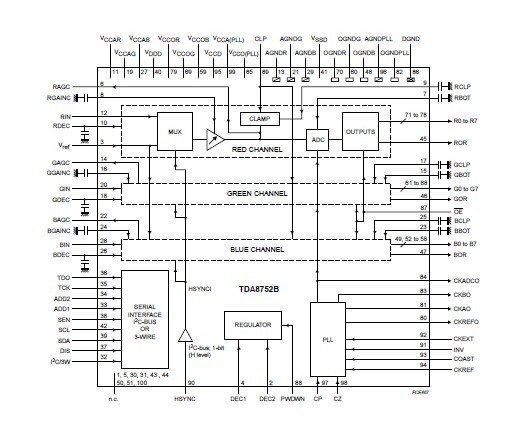
The TDA8752BH is a triple 8-bit ADC with controllable amplifiers and clamps for the digitizing of large bandwidth RGB signals. The clamp level, the gain and all of the other settings are controlled via a serial interface (either I2C-bus or 3-wire serial bus, selected via a logic input). The IC also includes a PLL that can be locked to the horizontal line frequency and generates the ADC clock. The PLL jitter is minimized for high resolution PC graphics applications. An external clock can also be input to the ADC. It is possible to set the TDA8752BH serial bus address between four fixed values, in the event that several TDA8752BH ICs are used in a system, using the I2C-bus interface (for example, two ICs used in an odd/even configuration).
Parametrics
TDA8752BH absolute maximum ratings: (1)VCCA analog supply voltage: -0.3 +7.0 V; (2)VCCD digital supply voltage: -0.3 +7.0 V; (3)VDDD logic input voltage: -0.3 to +7.0 V; (4)VCCO output stages supply voltage: -0.3 to +7.0 V; (5)DVCC supply voltage differences; (6)Vi(RGB) RGB input voltage range referenced to AGND: -0.3 to +7.0 V; (7)Io output current: - 10 mA; (8)Tstg storage temperature: -55 to +150 ℃; (9)Tamb ambient temperature: 0 to 70 ℃; (10)Tj junction temperature: - 150 ℃.
Features
TDA8752BH features: (1)Triple 8-bit ADC; (2)Sampling rate up to 110 MHz; (3)IC controllable via a serial interface, which can be either I2C-bus or 3-wire, selected via a TTL input pin; (4)IC analog voltage input from 0.4 to 1.2 V (p-p) to produce a full-scale ADC input of 1 V (p-p); (5)3 clamps for programming a clamping code between -63.5 and +64 in steps of 1/2LSB; (6)3 controllable amplifiers: gain controlled via the serial interface to produce a full scale resolution of 1/2LSB; (7)peak-to-peak; (8)Amplifier bandwidth of 250 MHz; (9)Low gain variation with temperature; (10)PLL, controllable via the serial interface to generate the ADC clock, which can be locked to a line frequency of 15 to 280 kHz; (11)Integrated PLL divider; (12)Programmable phase clock adjustment cells; (13)Internal voltage regulators; (14)TTL compatible digital inputs and outputs; (15)Chip enable high-impedance ADC output; (16)Power-down mode; (17)Possibility to use up to four ICs in the same system,using the I2C-bus interface, or more, using the 3-wire serial interface; (18)1.1 W power dissipation.
Diagrams
 |
 TDA8000 |
Other |
|
Data Sheet |
Negotiable |
|
||||
|
TDA8000T |
Other |
|
Data Sheet |
Negotiable |
|
||||
|
TDA8001 |
Other |
|
Data Sheet |
Negotiable |
|
||||
|
TDA8002 |
Other |
|
Data Sheet |
Negotiable |
|
||||
|
TDA8002C |
Other |
|
Data Sheet |
Negotiable |
|
||||
|
TDA8002C/CD |
NXP Semiconductors |
I/O Controller Interface IC SMRT CRD INTERFCE IC |
Data Sheet |
Negotiable |
|
||||